


Automotive
Micro Vehicles and the Future
As the name suggests, micro vehicles is a term used to loosely describe vehicles that are typically below 1100 pounds – 500 kilograms in metric terms – and operate at speeds below 25 kilometers per hour or 15 miles an hour.
Some perfect examples would include bicycles, skateboards, electric scooters, electric bikes among many others.
What is Micromobility?
By definition, micromobility refers to the use of micro vehicles which, as described above, are lightweight vehicles typically below 500 kilos. Micromobility has become quite popular of late in major cities and otherwise all over the world.
They are particularly very handy in navigating those vintage, old towns with narrow streets – whose architecture is just breathtaking I might add.
Have you ever thought of just riding up to work or going to the store to get some groceries on your bike or scooter for that matter? If no I would suggest having a go at it for, well a couple of reasons.
Reasons for Using Micromobility
Cheap mode of travel
It doesn’t get any cheaper than just hopping onto your bike or skateboard and just riding away to wherever you are going. If anything, you would only have to pay your legs for cycling you there. For the modes that you would have to pay for like e-bikes and e-scooters, it still is considerably cheaper than using a cab or riding the bus.
Convenient and fast
There literally are zero logistics involved in getting on a bike and you certainly do not need any special skills bar knowing how to ride a bike which I must say is not that special a skill. Convenience comes in when navigating heavy traffic and you can just seamlessly weave your way through along cycling lanes.
Environmental-friendly
This is owing to the fact that they have zero carbon emission with no fossil fuels being burnt and you can be on your merry way without worrying about damaging mother earth’s ozone layer which in truth is keeping us alive. With many people now conscious about saving our mother planet, micromobility has been the way to go.
Safety
One of the major reasons for the popularity gained by micromobility is its safety. The odds of crashing to death on your bike because you were speeding are far much lower than when using other means of transport.
That said, however, to absolutely achieve safe micromobility, other road users, pedestrians, and motorists alike have to be at the top of their game with regard to following traffic rules and what not.
Accidents Today
In the modern day, accidents have sadly been more common than any of us would have preferred. These accidents are however preventable depending on the nature of what causes them. For instance, after a night out with your squad it is common knowledge that absolutely under no circumstances should you get behind the wheel, right? Well, turns out that knowledge is not that common after all, and – long story short – lives are lost and lots of damage caused, needlessly so.
Even without man, accidents still do happen with respect to autonomous cars also called self-driving cars.
Prevention? Better Than Cure
Besides finding a cure to utter human ignorance, the marvel that is science has found some ways to curb this plague.
Regardless of the programming that goes on, no disrespect to engineers, there is no algorithm that can predict a ball rolling onto the road and a kid running after it right in front of a self-driving car. Self-driving cars as it is have countless sensors to perceive their surroundings. That said, some functionalities are impossible to execute such as seeing round a bend and that is where v2x comes in a safe micromobility platform.
Vehicle to Everything
Somewhere in a perfect alternate world, vehicles are able to communicate with virtually anything that affects them as an entity and this perfect alternate world will be the reality of our world soon.
Taking that into account, vehicle to everything is a communication between a vehicle and any other entity that may affect or may be affected by the vehicle itself.
It amalgamates other specific types of communications as discussed below:
Vehicle to network or V2N
Refers to when a vehicle accesses the network for cloud-based services. It is also referred to as vehicle-to-cloud or V2C.
Vehicle to infrastructure or V2I
It is the exchange of data between a vehicle and roadside units. A roadside unit refers to equipment that is installed alongside roads.
A sample use of this is broadcasting traffic conditions to drivers.
Vehicle to vehicle or V2V
It is the transfer of data or information between vehicles. It offers a little more than basic sensors in the sense that information can be transmitted to and from a couple of hundred meters away or even through barriers like a truck in between the vehicles.
Vehicle to pedestrian or V2P
It is the exchange of data between cars and pedestrians.
How v2x Works As a Safe Micromobility Platform
In a vehicle-to-everything system, vehicles use their sensors to send data using high-bandwidth and high-reliability links. Each individual car has a sensor that sends data to other vehicles or infrastructure such as traffic lights and parking spaces.
Information shared is about surrounding entities such as weather conditions, traffic conditions, nearby accidents, road works notices among others. Information of this nature enhances the driver’s awareness of what surrounds them, which, in retrospect, reduces the chances of accidents all the while improving traffic efficiency.
As technologies varies in practically everything, this is no different and as a result, there are two classes.
Dedicated short-range communication
DSRC links two senders that are in close proximity to each other enabling them to communicate without the need for a specific communication device. The fact that no specific device is needed for communication makes it suitable for less developed areas.
It operates in short-range that is distances less than one kilometer and runs in the unlicensed 5.9 GHZ band. DRSC provides basic information like accident notices and toll payments.
DRSC is completely unaffected by weather conditions however harsh which essentially means even in times of heavy rains or snow, it still can scan the environment and deliver accurate data.
Cellular vehicle to everything communication
It is an alternative to DSRC that uses LTE as the chief fundamental technology. LTE, an acronym for Long Term Evolution, is a standard broadband communication for mobile devices and data terminals.
Vehicle-to-everything technology is an engineering marvel that allows vehicles to communicate with their surroundings as well as with each other over distances of about a mile. Here are some advantages.
Time saving
Traffic jams are basically the reason people are late to places in major urban areas and with this technology, vehicles can communicate with roadside units like traffic lights and traffic management systems which could allow for the prediction of the best route to take.
Convenience for drivers
Nothing is more calming to any driver really than knowing what is up ahead or knowing beforehand the traffic situation so they can avoid congested areas.
Enhanced traffic safety
With the capabilities this technology has, road accidents are greatly avoided with the information transmitted such as a notification that the car right up ahead is braking so you can be prepared to brake as well.

Automotive
The Rise of System-in-Package (SiP): How Advanced IC Packaging Is Redefining Electronics Miniaturization
Summary: System-in-Package (SiP) technology is one of the fastest-growing segments in semiconductor packaging, driven by demand for compact, high-performance devices across healthcare, defense, aerospace, and consumer electronics.
This article covers: what SiP is and why it matters; key market trends and drivers; the technical challenges facing engineers; the landscape of existing solutions; and how an all-in-one manufacturing approach delivers a competitive edge in SiP design and production.
As electronics continue to shrink while demands for performance grow, the industry faces a pivotal inflection point. For engineers and product teams researching IC packaging companies capable of delivering complete SiP solutions, understanding the full technology landscape has never been more important.
What Is System-in-Package and Why Does It Matter?
System-in-Package (SiP) is a technology approach that integrates multiple functional components – processors, memory, sensors, RF modules, and passive components – into a single compact package. Unlike a System-on-Chip (SoC), which integrates all functions onto a single die, SiP combines multiple dies and components, often using different process nodes, into one unified module.
This heterogeneous integration approach offers a powerful alternative to traditional multi-chip designs, addressing the core engineering tradeoffs of size, performance, power consumption, and cost. As consumer electronics, wearables, industrial IoT devices, and defense electronics demand ever-smaller form factors without sacrificing functionality, SiP has emerged as a foundational technology for the next generation of electronic systems.
Market Trends Driving SiP Adoption
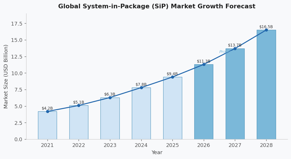
The global SiP market is on a steep growth trajectory. According to industry research, the market was valued at approximately $8 billion in 2024 and is forecast to approach $17 billion by 2028, growing at a compound annual rate exceeding 15%. Several macro trends are powering this expansion:
- IoT and Wearable Devices: The explosion of connected devices demands ultra-compact, low-power modules. SiP allows designers to integrate sensing, processing, and connectivity functions into a package small enough for a smartwatch or medical implant.
- 5G and Advanced Communications: Millimeter-wave 5G systems require highly integrated RF front-end modules. SiP enables the co-packaging of RF components with antenna structures, dramatically reducing signal loss and board real estate.
- Defense and Aerospace Miniaturization: Modern defense electronics – from drone guidance systems to soldier-worn electronics – require extreme miniaturization alongside ultra-high reliability under harsh environmental conditions.
- Medical Device Innovation: Implantable devices, hearing aids, and continuous health monitors are pushing miniaturization to new extremes, where SiP technology enables life-critical functionality in sub-centimeter packages.
- Automotive Electronics: Advanced driver-assistance systems (ADAS) and autonomous vehicle platforms require high-density, thermally reliable SiP modules capable of operating across extreme temperature ranges.
The Technical Challenges of SiP Design and Manufacturing
While SiP offers compelling advantages, its design and manufacturing complexity is substantial. Engineers face a constellation of technical challenges that require deep, cross-domain expertise:
- Thermal Management: Integrating multiple high-power components into a small package concentrates heat significantly. Ensuring reliable thermal dissipation without increasing package height or weight requires sophisticated substrate engineering, embedded coin technology, and careful die placement.
- Signal Integrity and Electromagnetic Interference (EMI): Heterogeneous integration creates complex signal routing challenges. Fine-pitch interconnects between dies must maintain controlled impedance while minimizing crosstalk and EMI – particularly critical in RF and high-speed digital applications.
- CTE Mismatch: Different materials – silicon dies, organic substrates, and passive components – expand and contract at different rates under thermal cycling. Managing coefficient of thermal expansion (CTE) mismatches is essential for long-term reliability, especially in aerospace and defense applications where temperature extremes are the norm.
- Supply Chain Complexity: Traditional SiP development requires coordinating multiple specialized vendors for substrate fabrication, die sourcing, assembly, and testing. Each handoff introduces risk, delay, and potential quality variation.
- Design for Testability: Testing a fully assembled SiP module is fundamentally more difficult than testing individual components. Embedded dies and multi-layer substrates limit physical access, requiring sophisticated In-Circuit Testing (ICT) and system-level test strategies.
The Landscape of SiP Solutions Today
The market has responded to SiP complexity in several ways. Large Outsourced Semiconductor Assembly and Test (OSAT) companies offer high-volume SiP assembly, but their minimum order quantities and standardized processes are often mismatched with the prototype-to-mid-volume needs of defense, aerospace, and medical device companies. Dedicated substrate foundries provide advanced substrate technology but require separate assembly and test partners, fragmenting the supply chain.
The result is that many engineering teams face a frustrating choice: accept the limitations of standardized, high-volume OSAT services, or manage a complex multi-vendor supply chain that introduces quality risk and schedule uncertainty. A third path – working with an integrated, all-in-one solutions provider – is increasingly recognized as the most effective approach for complex, high-reliability SiP programs.
For a deeper understanding of the academic and technical foundations of SiP development, the IEEE Xplore library provides extensive peer-reviewed research on heterogeneous integration, organic substrates, and advanced packaging reliability testing.
How an All-in-One Approach Addresses SiP Complexity
PCB Technologies, with its specialized iNPACK division, has built an integrated capability that directly addresses the core challenges of SiP development. As described on their website, the company is an “All-in-One Solutions Provider of Miniaturization & Advanced IC Packaging Solutions,” operating with a single-roof approach that spans design, substrate fabrication, package assembly, and testing.
Their iNPACK division offers advanced System-in-Package solutions as multi-component, multifunction products. Key capabilities include size reduction, high thermal conductivity, ultra-thin substrates with fine lines and spacing, controlled CTE, 3D design, shielding options, sealing solutions, fine-pitch flip-chip and copper pillar technology, double-side assembly, development and production testing, and full turnkey solutions.
A core differentiator of iNPACK is its organic substrate technology, supporting 25-micron lines and 25-micron spacing – precision that enables the fine-pitch signal routing critical to advanced SiP applications. Their on-site, certified cleanroom manufacturing facility ensures that sensitive components remain free from contamination throughout the assembly process.
Critically, PCB Technologies’ approach eliminates the multi-vendor fragmentation that plagues many SiP programs. Their R&D center is located within the same complex as their manufacturing facilities, enabling seamless transitions from design iteration to prototype production without the handoff delays and communication gaps inherent in fragmented supply chains.
For engineers exploring panel level packaging as an alternative to wafer-level processes, iNPACK’s panel-level approach uses rectangular panels similar to organic substrate manufacturing – designed for efficient production, lower cost per unit, and the flexibility to incorporate Multi-Chip Module (MCM) and SiP assembly on the same production infrastructure.
SiP in Practice: Applications Across High-Demand Industries
The industries best positioned to leverage SiP technology share a common need: maximum functionality in minimum space, with uncompromising reliability. PCB Technologies serves customers across medical, defense, aerospace, communications, and semiconductor sectors – all of which are increasingly turning to SiP as a strategic platform.
- Defense Electronics: Miniaturized radar modules, electronic warfare systems, and soldier-worn communications devices require SiP solutions that maintain performance under shock, vibration, and extreme temperatures. High-reliability SiP with embedded thermal management meets these requirements.
- Medical Devices: From cochlear implants to continuous glucose monitors, medical SiP modules must combine RF, sensing, and processing in biocompatible packages that meet ISO 13485 quality standards – a certification held by PCB Technologies.
- IoT and Industrial Systems: Industrial IoT nodes that operate in harsh environments require rugged SiP modules with wide operating temperature ranges, integrated sensing, and low-power wireless connectivity.
Conclusion: SiP Is No Longer Optional — It Is a Strategic Imperative
System-in-Package technology has moved from a niche solution for space-constrained applications to a mainstream platform technology across multiple high-growth industries. For product teams facing the dual pressure of miniaturization and performance, SiP is increasingly the answer – but only when implemented with the right combination of substrate expertise, assembly precision, and integrated design-to-test capability.
The companies that will lead in the next wave of electronics miniaturization will be those that choose manufacturing partners capable of delivering SiP solutions as an end-to-end, accountable service – from substrate design through final system testing, all under one roof.
Summary: IC interconnect technology – how a semiconductor die connects electrically to its substrate or package – is one of the most consequential decisions in modern electronics design.
This article examines: the technical fundamentals of wire bonding and flip chip packaging; the market trends reshaping interconnect technology choices; the engineering tradeoffs that determine which approach is optimal for a given application; the landscape of available solutions; and how an integrated packaging capability enables engineers to access both technologies – and choose freely between them – within a single supply chain.
For engineers evaluating interconnect strategies for their next design, understanding the full depth of wire bonding options and their flip chip alternatives is essential. The choice directly affects device performance, package size, signal integrity, manufacturing cost, and qualification timeline.
The Fundamentals: What Wire Bonding and Flip Chip Actually Are
At its core, the IC interconnect challenge is straightforward: a semiconductor die contains hundreds or thousands of tiny electrical contact pads. Those pads must be connected to the package substrate – which then connects to the PCB – with minimal resistance, inductance, and crosstalk, while maintaining mechanical integrity through thermal cycling, vibration, and shock.
Wire Bonding is the oldest and most widely used interconnect technique. Thin wires – typically gold, copper, or aluminum – are bonded from the die bond pads to the package substrate using thermal compression, ultrasonic energy, or a combination of both (thermosonic bonding). The resulting wire loops are visible under a microscope as delicate arcs spanning from die to substrate.
Flip Chip packaging inverts this approach. Instead of bonding wires from the top surface of the die, the die is flipped face-down, with solder bumps or copper pillars on the active surface connecting directly to matching pads on the substrate. The entire connection is made through these bumps in a single reflow step, with no wire loops.
Market Trends: The Steady Rise of Flip Chip
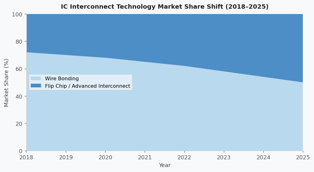
The global IC packaging market is undergoing a structural shift away from wire bonding as the dominant interconnect approach, driven by the performance demands of advanced applications. Industry research indicates that flip chip packaging now accounts for roughly half of the total IC interconnect market by value, with penetration continuing to grow in high-performance segments.
Several converging trends are driving this shift:
- High-Speed Digital Performance: Modern processors, memory controllers, and network chips operate at speeds where wire inductance – an inherent characteristic of wire bond loops – causes signal integrity problems. Flip chip’s shorter, lower-inductance interconnects are essential for chips operating above a few gigahertz.
- Fine-Pitch I/O Requirements: As die complexity increases, the number of I/O connections grows and their pitch shrinks. Advanced chips now require hundreds to thousands of I/O connections at pitches that wire bonding cannot reliably achieve, but flip chip copper pillars can support.
- Thermal Performance: Flip chip’s inverted die placement exposes the back side of the silicon directly upward, enabling direct attachment of a heatsink to the die – dramatically improving thermal dissipation compared to wire bonded packages where the die back faces the substrate.
- Package Height Reduction: Wire bond loops require vertical clearance above the die. Flip chip eliminates this requirement, enabling ultra-thin packages critical for wearables, implantable medical devices, and ultra-thin consumer electronics.
Where Wire Bonding Remains the Optimal Choice
Despite the growth of flip chip, wire bonding is far from obsolete – and for many applications, it remains the technically and economically optimal choice.
- Cost-Sensitive, Standard I/O Applications: Wire bonding equipment and processes are mature, widely available, and highly cost-effective for chips with moderate I/O counts and standard pitch. For commodity sensors, microcontrollers, and discrete semiconductors, wire bonding delivers excellent performance at minimal cost.
- Mixed-Die Assemblies: In multi-chip module (MCM) designs and System-in-Package (SiP) assemblies, wire bonding enables flexible interconnection between dies of different sizes and heights – including die-to-die connections within the same package that would be impractical with bump-based approaches.
- Known-Good Die (KGD) Management: Wire bonding can be performed after functional testing of individual dies, reducing the risk of assembling expensive SiP modules with defective components.
- Rework Capability: Wire bonds can be selectively reworked – broken bonds can be re-bonded – providing a repair option that flip chip assemblies generally do not offer, which is valuable in low-volume, high-value applications.
Flip Chip vs. Wire Bond: The Engineering Decision Framework
The choice between flip chip vs wire bond is not a binary decision with a universal right answer. It is a multi-dimensional optimization across performance, cost, form factor, reliability, and supply chain complexity. The key decision drivers include:
- Operating Frequency: For applications below approximately 1 GHz, wire bonding is typically sufficient. For RF, mmWave, and high-speed digital applications above a few GHz, flip chip’s lower parasitics become essential.
- I/O Count and Pitch: For designs with more than a few hundred I/O at fine pitch, flip chip or copper pillar technology is generally required. Wire bonding becomes physically impractical at very high I/O densities.
- Package Thickness: For applications where vertical space is at a premium, flip chip eliminates the wire loop height overhead – typically 200–400 microns – enabling thinner packages.
- Thermal Requirements: High-power dies benefit significantly from the superior thermal path provided by direct heatsink attachment enabled by flip chip orientation.
- Volume and Cost Sensitivity: At low-to-medium volumes, wire bonding is typically more cost-effective. At high volumes, the economics become more application-specific and are influenced heavily by substrate cost, yield, and test strategy.
The Integration Advantage: Access to Both Technologies in One Supply Chain
One of the most underappreciated challenges in advanced IC packaging is the supply chain fragmentation that results when different interconnect technologies require different vendors. Many organizations source wire bonding from one assembly house, flip chip from another, and organic substrates from a third – creating a coordination burden that adds time, cost, and quality risk to every program.
PCB Technologies, through its iNPACK division, offers a fundamentally different model. As described in their materials, the iNPACK division provides complete package PCB assembly solutions including SiP design and manufacturing, surface mount technology, chip on board (COB) wire bonding, microfabrication, and substrate design and manufacturing – all under one roof.
Their substrate technology supports 25-micron lines and 25-micron spacing, enabling the fine-pitch routing required for both advanced wire bond fan-out designs and flip chip copper pillar interconnects. Their cleanroom manufacturing facility, certified to ISO 9001, ISO 14001, ISO 13485, and AS 9100, ensures the contamination control and process discipline required for reliable advanced interconnects.
For engineers seeking academic grounding in IC interconnect technologies, IEEE Xplore provides extensive peer-reviewed literature on wire bonding reliability, flip chip process development, and advanced packaging interconnect performance – an essential reference for teams evaluating interconnect technology choices.
The Path Forward: Heterogeneous Integration
The most sophisticated packaging programs today do not choose between wire bonding and flip chip – they use both, strategically, within the same SiP module. A high-power processor might use copper pillar flip chip interconnects for maximum performance, while peripheral functions such as a power management IC, a sensor die, or an RF module are wire bonded to the same substrate.
This heterogeneous integration approach requires the substrate to accommodate both interconnect types simultaneously, with the DfM expertise to ensure that both are manufacturable, testable, and reliable at production scale. It is a capability that demands deep, integrated expertise across substrate design, interconnect technology, assembly process, and test engineering.
Conclusion: The Right Interconnect for the Right Application
Wire bonding and flip chip packaging represent complementary – not competing – technologies in the modern IC packaging toolkit. The engineering challenge is not to choose one universally, but to understand each application’s specific requirements deeply enough to select the right approach, and to partner with a manufacturing organization capable of executing either strategy with equal precision and accountability.
As miniaturization continues to advance and new application categories – implantable medical devices, next-generation defense electronics, advanced automotive systems – push the boundaries of what is possible, the ability to access both interconnect technologies through a single, integrated supply chain will increasingly determine which organizations can deliver on their design intent.
Automotive
Automotive PCBs: Engineering Reliability for the Era of Autonomous and Electric Vehicles
Learn how pcb manufacturing processes support modern automotive electronics, enabling reliable performance for electric vehicles, ADAS systems, and autonomous driving technologies. This guide explores the PCB technologies, materials, and standards that power next-generation vehicles.
The modern automobile is no longer simply a mechanical machine. Today’s vehicles whether a conventional combustion engine car, a battery electric vehicle (BEV), or a fully autonomous system are deeply sophisticated electronics platforms. Every function, from the engine management system and power steering to the infotainment screen and lidar sensor array, depends on printed circuit boards engineered to perform reliably across extreme temperature ranges, severe vibration, and decades of continuous operation.
Automotive PCBs are among the most demanding products in the electronics manufacturing industry. Failure is not an option: a board that malfunctions in an automotive safety system can have life-altering consequences. This article explores the technology, standards, and applications that define automotive PCBs and explains why pcb-technologies is a trusted supplier to OEMs and their Electronic Manufacturing Services (EMS) providers worldwide.
Why Automotive PCBs Are Different
Automotive electronics must operate across temperature ranges from -40°C to 85°C or beyond, withstand continuous vibration and mechanical shock, resist moisture and chemical exposure, and maintain full performance for 15+ years of vehicle lifetime. Standard commercial PCBs are not designed for these demands.
The transition to electric and autonomous vehicles has intensified these requirements. New automotive PCB challenges include:
- Power electronics for EV drivetrains: High-current boards managing hundreds of amperes and hundreds of volts for motor inverters and charging systems
- AI processors for autonomous driving: Boards supporting AI accelerators (GPUs, TPUs) with Ball Grid Array packages requiring fine lines, micro-vias, and ultra-low-loss materials for data rates exceeding 25 Gbps
- Lidar and radar modules: High-frequency RF boards requiring specialized PTFE or ceramic-based laminates to maintain signal integrity at millimeter-wave frequencies
- ADAS sensor fusion: Multiple sensor types (radar, lidar, cameras, ultrasonic) integrated through high-density PCB interconnects
- In-cabin electronics: Touchscreens, heads-up displays, driver monitoring systems all requiring compact, reliable PCBs
Types of PCBs Used in Automotive Applications
pcb-technologies supplies multiple PCB types tailored to the specific demands of automotive electronics:
HDI PCBs (High-Density Interconnect)
HDI PCBs are ideal for automotive control technology, with the ability to pack more functionality into a smaller, lighter footprint. In an industry where size and weight are critical for fuel efficiency and EV range, HDI technology uses micro-vias and fine lines to enable complex, multi-layered designs that would be impossible on conventional boards. pcb-technologies produces HDI boards using the Excellon Cobra Hybrid Laser system and X-VIA technology for precise, void-free via structures.
Explore the iNPACK division for advanced packaging in automotive applications at pcb-technologies iNPACK.
Rigid-Flex PCBs
Combining the durability of a rigid board with the flexibility of a flex circuit, rigid-flex PCBs are perfect for automotive applications that require a design fitting into tight or irregularly shaped spaces such as steering column electronics, dashboard assemblies, and camera modules in door mirrors. Rigid-flex eliminates the need for bulky connectors and wire harnesses, reducing both weight and failure points.
RF Boards (Radio Frequency)
Modern vehicles depend on a growing number of RF systems: GPS, V2X (vehicle-to-everything) communications, LTE/5G telematics, radar-based ADAS systems, and keyless entry. RF boards require specialized materials like PTFE or ceramic-based laminates to maintain signal integrity and minimize loss at high frequencies. pcb-technologies has extensive expertise in RF board design and fabrication.
Thermal Management PCBs
Automotive electronics impose significant thermal loads, particularly in power electronics for EVs and high-performance engine control units. pcb-technologies combines materials science, mechanical engineering, and PCB manufacturing technology to effectively dissipate heat. Solutions include embedded copper coins, thermal vias, metal-core boards, and specialized thermally conductive laminates.
Learn more about pcb-technologies’ automotive PCB solutions at automotive industry page.
Automotive Quality Standards: IATF 16949 and Beyond
The automotive industry operates under some of the strictest quality management requirements in any sector. The key standard is IATF 16949, which defines quality management system requirements specifically for the design, development, production, installation, and service of automotive-related products.
pcb-technologies is certified to IATF 16949, along with a comprehensive suite of additional certifications relevant to automotive customers:
- IATF 16949 — Automotive quality management system
- ISO 9001 — General quality management
- ISO 14001 — Environmental management
- NADCAP — Defense and aerospace process accreditation (for defense-grade automotive programs)
- AS9100 — Aerospace quality management (relevant for autonomous vehicle programs with aerospace-grade requirements)
- RoHS Lead-Free compliance — Fully compliant with automotive RoHS requirements
- IPC-A-610 and J-STD-001 — Assembly standards for all PCBA
pcb-technologies’ Automotive PCB Capabilities
With over 40 years of experience in high-reliability PCB manufacturing, pcb-technologies has built a well-earned reputation in the automotive sector. Key capabilities include:
- Full design services: From initial schematic through DfM, DfT, DfP, DfC, and DfA analysis optimized for automotive quality and cost targets
- Advanced materials: Including Rogers laminates, PTFE, polyimide, and metal-core for specific automotive performance requirements
- High-current PCBs: Supporting relay and fuse boxes, DC/DC converters, inverters for EV systems, and power/signal integration on one board
- PCBA with advanced packaging: Including Package-on-Package (POP), Micro BGAs, and IC packaging services through the iNPACK division
- Comprehensive testing: ICT, AOI, functionality testing, and vibration testing (S452 Electrodynamic Shaker) critical for automotive reliability validation
- NPI (New Product Introduction): Fast-tracked NPI services supporting rapid development cycles typical in automotive Tier 1 and OEM programs
The Road Ahead: Automotive Electronics Trends
The automotive PCB market is in the midst of a fundamental transformation, driven by electrification and autonomy:
- Software-defined vehicles: Central computing architectures replacing distributed ECUs, requiring fewer but more powerful, high-density PCBs
- V2X (Vehicle-to-Everything): PCBs supporting 5G NR and DSRC communication modules for cooperative driving
- Integrated AI at the edge: Boards with AI accelerators running machine learning models for real-time visual quality control and autonomous decision-making
- Wearable and in-cabin electronics: Flexible and rigid-flex PCBs enabling new form factors for driver and passenger interfaces
- Battery Management Systems (BMS): High-reliability, high-current boards for EV battery pack management
pcb-technologies is positioned to serve all these emerging requirements, with its iNPACK miniaturization platform and comprehensive design-to-production capability ready for the automotive industry’s next decade.
Return to the pcb-technologies homepage at pcb-technologies.com.
Frequently Asked Questions
Q: What certifications does pcb-technologies hold for automotive PCBs?
A: pcb-technologies is certified to IATF 16949 (automotive), ISO 9001, ISO 14001, NADCAP, AS9100, and RoHS. All assembly is performed by IPC-A-610 and J-STD-001 certified experts.
Q: What types of PCBs are used in electric vehicles?
A: EV applications use HDI PCBs (for ADAS and control electronics), RF boards (for telematics and radar), thermal management PCBs (for power electronics and battery management), rigid-flex PCBs (for compact form factors), and high-current boards for inverters, converters, and battery management systems.
Q: Why is thermal management critical for automotive PCBs?
A: Automotive electronics generate significant heat, especially in EV power electronics and AI processors. Boards that cannot dissipate heat reliably will fail prematurely — a safety-critical issue. Thermal management solutions include embedded copper coins, thermal vias, metal-core boards, and specialized laminates.
Q: What is IATF 16949 and why does it matter?
A: IATF 16949 is the international automotive quality management standard. It covers design, development, production, installation, and service of automotive-related products. Automotive OEMs and Tier 1 suppliers typically require their PCB manufacturers to be IATF 16949 certified.
Q: Can pcb-technologies produce automotive PCB prototypes as well as production volumes?
A: Yes. pcb-technologies supports the full product lifecycle from NPI prototype through low, mid, and high volume production — all with the same quality standards and certifications.

Edge AI Explained: How On-Device AI Processing Is Replacing the Cloud
The Rise of System-in-Package (SiP): How Advanced IC Packaging Is Redefining Electronics Miniaturization
Wire Bonding vs. Flip Chip: Navigating the Evolving World of IC Interconnect Technology

-
Business Solutions2 years ago
Understanding A2P Messaging and the Bulk SMS Business Landscape
-

 Business Solutions2 years ago
The Power of Smarts SMS and Single Platform Chat Messaging
-

 Business Solutions2 years ago
Exploring OTP Smart Features in Smart Messaging Services
-

 Business Solutions2 years ago
Live Video Broadcasting with Bonded Transmission Technology
-

 Business Solutions1 year ago
The Future of Healthcare SMS and RCS Messaging
-

 Business Solutions2 years ago
2-Way Texting Solutions from Company Message Services
-

 Business Solutions2 years ago
Communication with Analog to Fiber Converters & RF Link Budgets
-

 Business Solutions2 years ago
B2B vs. B2C Content Creation: Tailoring Your Message to Win the Deal