


Industrial Solutions
Emergency Management Solution for Mining 4.0 Deployment and Operational Risk Management
Mining 4.0 ushers in a new era of mining operations, bringing substantial innovation to the industry that promises greater efficiency and security. As such, emergency management planning for Mining 4.0 deployment and operational risk has never been more important – and more complex than ever. In this blog post, we will examine the strategies which organizations must consider when looking to adapt their emergency response plans for protection against potential threats from Mining 4.0 adoption and provide advice on how best to navigate these challenges with an effective solution for mining 4.0 emergency management planning.
Technology has always played a role in mining, but the industry is now on the edge of a new era – Mining 4.0. This fourth industrial revolution is set to change the way we mine forever, starting with emergency management. Mining 4.0 uses technology to increase efficiency, reduce waste, and improve safety and security throughout the mining life cycle. And while there are many benefits to this new way of mining, there are also risks that come with it. This blog post will explore how an emergency management solution can help you deploy Mining 4.0 while managing operational risk. We will also look at some challenges you may face and how to overcome them.
Operational risk management
Operational risk management is identifying, assessing, and managing risks that could impact an organization’s operating performance. In the mining industry, operational risks can include environmental hazards and equipment failures.
An effective emergency management solution for mining operations must consider all potential operational risks and have a plan to mitigate them. To do this, mines need to comprehensively understand their specific risks and what steps must be taken to prevent or reduce the impact of those risks.
Operational risk management or ORM software starts with identifying all potential sources of risk. Once identified, each risk should be assessed in terms of its likelihood and potential impact on operations. Once all risks have been identified and evaluated, mines can develop mitigation plans to address each one.
The goal of an emergency management solution for mining is to protect workers, equipment, and the environment from harm. By identifying and assessing all potential sources of operational risk, mines can develop comprehensive mitigation plans that will help keep their operations safe and running smoothly.

Mining 4.0 Implementation and Operational Risk Management
Mining 4.0 is the fourth industrial revolution in mining and is achieved by applying digital technology to all mining operations. The smart mine is a connected mine where digital technologies manage every aspect of functions, from exploration and geology to mining, processing, and logistics.
Mining 4.0 has the potential to deliver significant value for miners through increased productivity, safety, and sustainability. However, the successful implementation of Mining 4.0 requires a step change in how mines are operated and managed. This means a new approach to risk management is needed, one that takes into account the complexities of operating a digital mine.
Operational risk management is the process of identifying, analyzing, and mitigating risks that could harm your company. It is an essential part of any organization’s overall risk management strategy and helps ensure that risks are identified early and managed effectively.
The successful implementation of Mining 4.0 will require a comprehensive ORM system that takes into account all aspects of digital transformation. This includes risks associated with new technology implementations, changes to business processes and organizational structures, and reputational risks related to data breaches or cyber-attacks.
An effective ORM system will help miners identify, assess and manage these risks throughout the lifecycle of their Mining 4.0 initiatives. It will also assure stakeholders that risks are managed effectively, and those objectives are achievable.
The Problem: Poor Emergency Management in the Mining Industry
Mining is one of the world’s highest levels of dangerous occupations. Poor emergency management can lead to disastrous consequences, including loss of life, injuries, and property damage.
Many factors contribute to poor emergency management in the mining industry. One major factor is the dispersed nature of mining operations. Mines are often located in remote areas, making it difficult for emergency responders to reach them promptly. Additionally, mines are usually found in hazardous environments, such as near volcanoes or flood-prone regions. This can make it difficult to evacuate miners in an emergency.
Another factor contributing to poor emergency management in the mining industry is the high risk associated with mining operations. Mining is a dangerous profession, and accidents are not uncommon. In fact, according to the Mine Safety and Health Administration (MSHA), there were 861 mining fatalities between 2006 and 2015. This high rate of accidents makes it difficult for emergency responders to compete with the demand for their services.
Finally, many mining companies need to have adequate plans or resources in place to deal with emergencies. This lack of preparedness can lead to chaotic and disorganized responses to emergencies, making them even more dangerous.
Emergency management is critical to keeping miners safe and protecting property during mining operations. However, due to the unique challenges associated with the mining industry, it can take time to implement effective emergency management strategies.
The Solution: Emergency Management Software
Many commercial off-the-shelf emergency management software (COTS) solutions are available today. But, finding the right one that meets the specific needs of the mining industry can take time and effort.
When considering a COTS solution for mining, it is essential to keep in mind the unique challenges of managing emergencies in this industry. These challenges include:
- The need to manage large amounts of data and information
- The need for real-time collaboration between multiple stakeholders
- The need to integrate with other systems and applications
- The need for flexibility and customization
With these challenges in mind, here are five things to look for in an emergency management solution for mining:
- Data Management: Look for a solution to help you manage large amounts of data, including incident data, asset data, weather data, and more. The answer should also offer reporting capabilities to track trends and patterns over time.
- Real-Time Collaboration: In an emergency, time is of the essence. Look for a solution that offers real-time collaboration features so multiple stakeholders can work together to resolve the issue as quickly as possible.
- Integration: A good emergency management solution should be able to combine with other systems and applications, such as GIS systems, asset management systems, and weather forecasting systems. This will give you a complete picture of what is happening during an emergency and help you make better decisions.
- Flexibility and Customization: Look for a flexible solution that can be customized to meet your specific needs. This will ensure that the solution works how you need it to and grows with your organization over time.
- Support: When considering an emergency management solution, consider the vendor’s support offerings. In an emergency or disaster, you need to know that you can count on the vendor to provide timely support and assistance.
Solution for mining 4.0 deployment
Mining 4.0 is the next step in the digital transformation of the mining industry. It combines advanced technologies such as the Internet of Things (IoT), Big Data and Analytics, 3D Printing, and Robotics and Automation to create a more connected, automated, and efficient mining operation.
Mining Industry 4.0 is an innovative approach to mining that combines sensors and data analytics to identify potential safety hazards before they become an issue. Mining 4.0 has the potential to drastically improve safety and efficiency in mining operations while reducing costs. In addition, by automating repetitive tasks such as drilling and hauling, Mining 4.0 can help reduce accidents and injuries due to human error.
However, deploying Mining 4.0 can be challenging for many organizations due to the high upfront investment required and the need for specialized skill sets. Additionally, operational risks such as cyber security threats must be managed effectively to protect against disruptions to the business.
Emergency management software
Mining is a high-risk industry, and emergency management is critical to protecting workers, the environment, and company assets. An effective emergency management solution must provide visibility into all aspects of the operation, from the location of personnel and equipment to real-time data on weather and environmental conditions. It must also offer response tools for quickly mobilizing resources and coordinating response efforts.
Emergency management software offers all of these capabilities and more. The platform enables you to create a comprehensive emergency management plan that considers all potential hazards at your mine site. It also offers a suite of response tools that allow you to rapidly deploy resources and organize response efforts in the event of an incident. And because the platform is cloud-based, you can access it from anywhere – even in the most remote locations.
Mining 4.0 is an exciting new development in the industry, but it also comes with its unique set of risks and challenges. An emergency management solution designed explicitly for Mining 4.0 can help mitigate these risks and ensure a safe and successful deployment of this new technology. Such a solution can provide real-time critical infrastructure monitoring, streamlined communication between all stakeholders, and comprehensive risk management capabilities. To avoid any potential disasters, it is essential to have an emergency management solution in place before deploying Mining 4.0.


Edge AI Explained: How On-Device AI Processing Is Replacing the Cloud
The phrase ‘AI in the cloud’ dominated the technology conversation for most of the past decade. But for a growing number of applications – autonomous vehicles, industrial inspection, smart cameras, medical devices – cloud latency and connectivity dependence are not acceptable constraints. The answer is edge AI: the practice of running AI inference directly on the device generating the data.
This shift is not incremental. It represents a fundamental rethinking of where intelligence lives in a computing system. Understanding the architecture, tradeoffs, and hardware that enables edge AI is essential for any engineer or product team building AI-powered systems today.
Figure 1: Edge AI vs. Cloud AI – relative performance across latency, privacy, cost, and offline capability, plus 2025–2026 deployment mix shift.
What Is Edge AI?
Edge AI refers to AI inference performed locally – on a device at or near the data source – rather than on a remote server or cloud platform. The ‘edge’ is defined by proximity to the data: a camera, a robot, a vehicle, a medical monitor.
The core operation in edge AI is inference: feeding data through a trained neural network to produce a prediction, classification, or detection result. Training these models still typically happens in the cloud using large GPU clusters. But once trained, the model can be compiled and optimized to run on purpose-built edge hardware.
Why ‘AI at the Edge’ Is Gaining Momentum
Three converging forces are driving the move from cloud to edge:
- Latency requirements: Applications like autonomous driving, industrial safety systems, and augmented reality require decisions in milliseconds. Round-trip latency to a cloud data center cannot reliably achieve this.
- Connectivity constraints: Many edge environments – factories, agricultural fields, underground infrastructure – have unreliable or absent internet connectivity. Cloud-dependent AI is not viable here.
- Data privacy and sovereignty: Regulations in healthcare, finance, and government increasingly restrict where data can be processed. On-device inference ensures that sensitive data never leaves the physical device.
The economics have also shifted. The cost of purpose-built edge AI silicon has dropped significantly, while cloud inference costs scale with usage. For high-frequency inference tasks – such as analyzing every frame from a hundred cameras – the break-even point strongly favors edge processing.
The Hardware That Makes Edge AI Possible
Not all processors are suited to AI inference. Running a modern object detection network on a general-purpose CPU is feasible but inefficient. Dedicated AI accelerators solve this through hardware architecture designed for the matrix multiplication and convolution operations that dominate neural network computation.
| Hardware Type | Architecture | Typical Use Case | TOPS Range |
| General CPU | Sequential / SIMD | Low-throughput inference | < 1 TOPS |
| GPU (embedded) | Parallel CUDA cores | Flexible, power-intensive | 1–10 TOPS |
| Dedicated AI Accelerator | Dataflow / systolic arrays | High-efficiency inference | 10–50+ TOPS |
| Vision Processing Unit | Fused vision + AI pipeline | Camera-integrated applications | 5–30 TOPS |
Purpose-built AI accelerators such as the Hailo-8 AI Accelerator deliver significantly higher TOPS-per-watt than GPU-based alternatives – a critical metric for battery-powered or thermally constrained edge deployments.
Edge AI vs. Cloud AI: A Practical Comparison
| Dimension | Cloud AI | Edge AI |
| Latency | 50ms–2000ms (network dependent) | < 10ms |
| Privacy | Data transmitted externally | Data stays on-device |
| Offline | Not available | Full functionality |
| Model complexity | Unlimited (server resources) | Constrained by hardware |
| Cost model | Pay-per-inference, scales up | Fixed hardware investment |
| Best for | Batch processing, complex models | Real-time, latency-critical |
Software: The Missing Piece in Edge AI Deployments
Hardware capability is only as useful as the software ecosystem surrounding it. Deploying a neural network to an edge device requires a compilation toolchain that translates the model – typically developed in PyTorch or TensorFlow – into an optimized binary for the target hardware.
The best edge AI platforms provide:
- A model compiler that handles quantization, layer fusion, and memory optimization automatically
- A runtime library for efficient inference execution
- Pre-compiled model libraries (model zoos) for common tasks
- Profiling tools to measure per-layer performance and identify bottlenecks
- Integration examples for popular platforms including Raspberry Pi, NVIDIA Jetson, and industrial SBCs
The Hailo AI Software Suite delivers this complete pipeline, making it possible to go from a PyTorch model to a running edge deployment with minimal platform-specific engineering. The Hailo Developer Zone provides documentation, tutorials, and pre-compiled models to accelerate time-to-deployment.
For a broader technical overview of edge AI architectures, IEEE Spectrum’s coverage of edge computing provides a solid reference point on where the industry is heading.
Real-World Edge AI Use Cases
The breadth of edge AI applications continues to expand. Current high-volume deployments include:
- Smart retail: People counting, queue detection, and product recognition running on in-store cameras without cloud dependency.
- Automotive ADAS: Driver assistance features – lane departure, pedestrian detection, sign recognition – all processed in-vehicle for safety-critical response times.
- Industrial quality control: Automated optical inspection on production lines, detecting defects at rates that exceed human inspection.
- Smart home and security: Object recognition, package detection, and intruder alerts running locally on home hubs or camera modules.
- Healthcare monitoring: Patient movement analysis and fall detection in care environments, with strict data privacy guarantees.
Conclusion
Edge AI is not a replacement for cloud computing – it is a complement that brings intelligence to where data is generated. For applications requiring real-time response, offline capability, or data privacy, it is now the architecturally correct choice.
For deeper technical coverage of how edge AI is reshaping industries, visit aitechpublication.medium.com for analysis from practitioners building these systems today.
Automotive
The Rise of System-in-Package (SiP): How Advanced IC Packaging Is Redefining Electronics Miniaturization
Summary: System-in-Package (SiP) technology is one of the fastest-growing segments in semiconductor packaging, driven by demand for compact, high-performance devices across healthcare, defense, aerospace, and consumer electronics.
This article covers: what SiP is and why it matters; key market trends and drivers; the technical challenges facing engineers; the landscape of existing solutions; and how an all-in-one manufacturing approach delivers a competitive edge in SiP design and production.
As electronics continue to shrink while demands for performance grow, the industry faces a pivotal inflection point. For engineers and product teams researching IC packaging companies capable of delivering complete SiP solutions, understanding the full technology landscape has never been more important.
What Is System-in-Package and Why Does It Matter?
System-in-Package (SiP) is a technology approach that integrates multiple functional components – processors, memory, sensors, RF modules, and passive components – into a single compact package. Unlike a System-on-Chip (SoC), which integrates all functions onto a single die, SiP combines multiple dies and components, often using different process nodes, into one unified module.
This heterogeneous integration approach offers a powerful alternative to traditional multi-chip designs, addressing the core engineering tradeoffs of size, performance, power consumption, and cost. As consumer electronics, wearables, industrial IoT devices, and defense electronics demand ever-smaller form factors without sacrificing functionality, SiP has emerged as a foundational technology for the next generation of electronic systems.
Market Trends Driving SiP Adoption
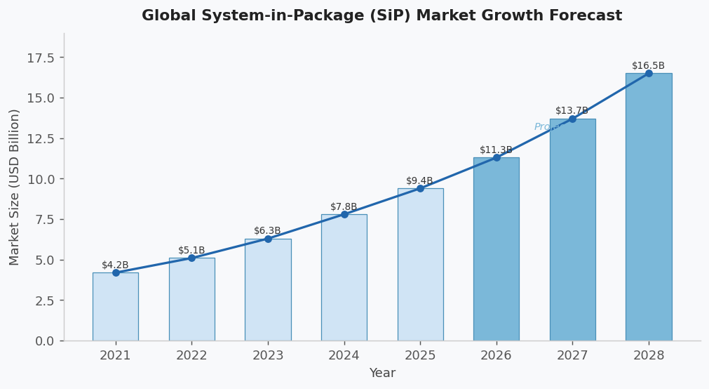
The global SiP market is on a steep growth trajectory. According to industry research, the market was valued at approximately $8 billion in 2024 and is forecast to approach $17 billion by 2028, growing at a compound annual rate exceeding 15%. Several macro trends are powering this expansion:
- IoT and Wearable Devices: The explosion of connected devices demands ultra-compact, low-power modules. SiP allows designers to integrate sensing, processing, and connectivity functions into a package small enough for a smartwatch or medical implant.
- 5G and Advanced Communications: Millimeter-wave 5G systems require highly integrated RF front-end modules. SiP enables the co-packaging of RF components with antenna structures, dramatically reducing signal loss and board real estate.
- Defense and Aerospace Miniaturization: Modern defense electronics – from drone guidance systems to soldier-worn electronics – require extreme miniaturization alongside ultra-high reliability under harsh environmental conditions.
- Medical Device Innovation: Implantable devices, hearing aids, and continuous health monitors are pushing miniaturization to new extremes, where SiP technology enables life-critical functionality in sub-centimeter packages.
- Automotive Electronics: Advanced driver-assistance systems (ADAS) and autonomous vehicle platforms require high-density, thermally reliable SiP modules capable of operating across extreme temperature ranges.
The Technical Challenges of SiP Design and Manufacturing
While SiP offers compelling advantages, its design and manufacturing complexity is substantial. Engineers face a constellation of technical challenges that require deep, cross-domain expertise:
- Thermal Management: Integrating multiple high-power components into a small package concentrates heat significantly. Ensuring reliable thermal dissipation without increasing package height or weight requires sophisticated substrate engineering, embedded coin technology, and careful die placement.
- Signal Integrity and Electromagnetic Interference (EMI): Heterogeneous integration creates complex signal routing challenges. Fine-pitch interconnects between dies must maintain controlled impedance while minimizing crosstalk and EMI – particularly critical in RF and high-speed digital applications.
- CTE Mismatch: Different materials – silicon dies, organic substrates, and passive components – expand and contract at different rates under thermal cycling. Managing coefficient of thermal expansion (CTE) mismatches is essential for long-term reliability, especially in aerospace and defense applications where temperature extremes are the norm.
- Supply Chain Complexity: Traditional SiP development requires coordinating multiple specialized vendors for substrate fabrication, die sourcing, assembly, and testing. Each handoff introduces risk, delay, and potential quality variation.
- Design for Testability: Testing a fully assembled SiP module is fundamentally more difficult than testing individual components. Embedded dies and multi-layer substrates limit physical access, requiring sophisticated In-Circuit Testing (ICT) and system-level test strategies.
The Landscape of SiP Solutions Today
The market has responded to SiP complexity in several ways. Large Outsourced Semiconductor Assembly and Test (OSAT) companies offer high-volume SiP assembly, but their minimum order quantities and standardized processes are often mismatched with the prototype-to-mid-volume needs of defense, aerospace, and medical device companies. Dedicated substrate foundries provide advanced substrate technology but require separate assembly and test partners, fragmenting the supply chain.
The result is that many engineering teams face a frustrating choice: accept the limitations of standardized, high-volume OSAT services, or manage a complex multi-vendor supply chain that introduces quality risk and schedule uncertainty. A third path – working with an integrated, all-in-one solutions provider – is increasingly recognized as the most effective approach for complex, high-reliability SiP programs.
For a deeper understanding of the academic and technical foundations of SiP development, the IEEE Xplore library provides extensive peer-reviewed research on heterogeneous integration, organic substrates, and advanced packaging reliability testing.
How an All-in-One Approach Addresses SiP Complexity
PCB Technologies, with its specialized iNPACK division, has built an integrated capability that directly addresses the core challenges of SiP development. As described on their website, the company is an “All-in-One Solutions Provider of Miniaturization & Advanced IC Packaging Solutions,” operating with a single-roof approach that spans design, substrate fabrication, package assembly, and testing.
Their iNPACK division offers advanced System-in-Package solutions as multi-component, multifunction products. Key capabilities include size reduction, high thermal conductivity, ultra-thin substrates with fine lines and spacing, controlled CTE, 3D design, shielding options, sealing solutions, fine-pitch flip-chip and copper pillar technology, double-side assembly, development and production testing, and full turnkey solutions.
A core differentiator of iNPACK is its organic substrate technology, supporting 25-micron lines and 25-micron spacing – precision that enables the fine-pitch signal routing critical to advanced SiP applications. Their on-site, certified cleanroom manufacturing facility ensures that sensitive components remain free from contamination throughout the assembly process.
Critically, PCB Technologies’ approach eliminates the multi-vendor fragmentation that plagues many SiP programs. Their R&D center is located within the same complex as their manufacturing facilities, enabling seamless transitions from design iteration to prototype production without the handoff delays and communication gaps inherent in fragmented supply chains.
For engineers exploring panel level packaging as an alternative to wafer-level processes, iNPACK’s panel-level approach uses rectangular panels similar to organic substrate manufacturing – designed for efficient production, lower cost per unit, and the flexibility to incorporate Multi-Chip Module (MCM) and SiP assembly on the same production infrastructure.
SiP in Practice: Applications Across High-Demand Industries
The industries best positioned to leverage SiP technology share a common need: maximum functionality in minimum space, with uncompromising reliability. PCB Technologies serves customers across medical, defense, aerospace, communications, and semiconductor sectors – all of which are increasingly turning to SiP as a strategic platform.
- Defense Electronics: Miniaturized radar modules, electronic warfare systems, and soldier-worn communications devices require SiP solutions that maintain performance under shock, vibration, and extreme temperatures. High-reliability SiP with embedded thermal management meets these requirements.
- Medical Devices: From cochlear implants to continuous glucose monitors, medical SiP modules must combine RF, sensing, and processing in biocompatible packages that meet ISO 13485 quality standards – a certification held by PCB Technologies.
- IoT and Industrial Systems: Industrial IoT nodes that operate in harsh environments require rugged SiP modules with wide operating temperature ranges, integrated sensing, and low-power wireless connectivity.
Conclusion: SiP Is No Longer Optional — It Is a Strategic Imperative
System-in-Package technology has moved from a niche solution for space-constrained applications to a mainstream platform technology across multiple high-growth industries. For product teams facing the dual pressure of miniaturization and performance, SiP is increasingly the answer – but only when implemented with the right combination of substrate expertise, assembly precision, and integrated design-to-test capability.
The companies that will lead in the next wave of electronics miniaturization will be those that choose manufacturing partners capable of delivering SiP solutions as an end-to-end, accountable service – from substrate design through final system testing, all under one roof.
Summary: IC interconnect technology – how a semiconductor die connects electrically to its substrate or package – is one of the most consequential decisions in modern electronics design.
This article examines: the technical fundamentals of wire bonding and flip chip packaging; the market trends reshaping interconnect technology choices; the engineering tradeoffs that determine which approach is optimal for a given application; the landscape of available solutions; and how an integrated packaging capability enables engineers to access both technologies – and choose freely between them – within a single supply chain.
For engineers evaluating interconnect strategies for their next design, understanding the full depth of wire bonding options and their flip chip alternatives is essential. The choice directly affects device performance, package size, signal integrity, manufacturing cost, and qualification timeline.
The Fundamentals: What Wire Bonding and Flip Chip Actually Are
At its core, the IC interconnect challenge is straightforward: a semiconductor die contains hundreds or thousands of tiny electrical contact pads. Those pads must be connected to the package substrate – which then connects to the PCB – with minimal resistance, inductance, and crosstalk, while maintaining mechanical integrity through thermal cycling, vibration, and shock.
Wire Bonding is the oldest and most widely used interconnect technique. Thin wires – typically gold, copper, or aluminum – are bonded from the die bond pads to the package substrate using thermal compression, ultrasonic energy, or a combination of both (thermosonic bonding). The resulting wire loops are visible under a microscope as delicate arcs spanning from die to substrate.
Flip Chip packaging inverts this approach. Instead of bonding wires from the top surface of the die, the die is flipped face-down, with solder bumps or copper pillars on the active surface connecting directly to matching pads on the substrate. The entire connection is made through these bumps in a single reflow step, with no wire loops.
Market Trends: The Steady Rise of Flip Chip
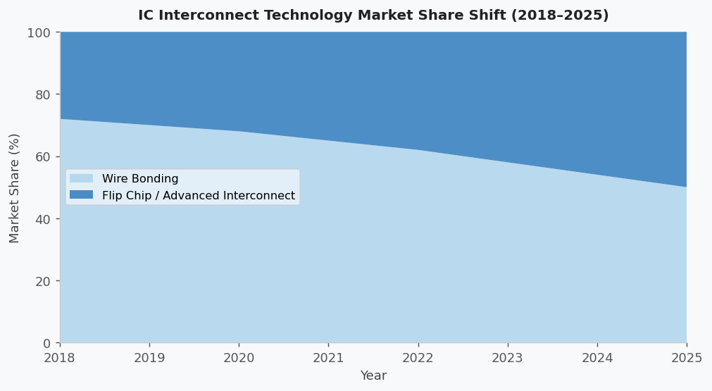
The global IC packaging market is undergoing a structural shift away from wire bonding as the dominant interconnect approach, driven by the performance demands of advanced applications. Industry research indicates that flip chip packaging now accounts for roughly half of the total IC interconnect market by value, with penetration continuing to grow in high-performance segments.
Several converging trends are driving this shift:
- High-Speed Digital Performance: Modern processors, memory controllers, and network chips operate at speeds where wire inductance – an inherent characteristic of wire bond loops – causes signal integrity problems. Flip chip’s shorter, lower-inductance interconnects are essential for chips operating above a few gigahertz.
- Fine-Pitch I/O Requirements: As die complexity increases, the number of I/O connections grows and their pitch shrinks. Advanced chips now require hundreds to thousands of I/O connections at pitches that wire bonding cannot reliably achieve, but flip chip copper pillars can support.
- Thermal Performance: Flip chip’s inverted die placement exposes the back side of the silicon directly upward, enabling direct attachment of a heatsink to the die – dramatically improving thermal dissipation compared to wire bonded packages where the die back faces the substrate.
- Package Height Reduction: Wire bond loops require vertical clearance above the die. Flip chip eliminates this requirement, enabling ultra-thin packages critical for wearables, implantable medical devices, and ultra-thin consumer electronics.
Where Wire Bonding Remains the Optimal Choice
Despite the growth of flip chip, wire bonding is far from obsolete – and for many applications, it remains the technically and economically optimal choice.
- Cost-Sensitive, Standard I/O Applications: Wire bonding equipment and processes are mature, widely available, and highly cost-effective for chips with moderate I/O counts and standard pitch. For commodity sensors, microcontrollers, and discrete semiconductors, wire bonding delivers excellent performance at minimal cost.
- Mixed-Die Assemblies: In multi-chip module (MCM) designs and System-in-Package (SiP) assemblies, wire bonding enables flexible interconnection between dies of different sizes and heights – including die-to-die connections within the same package that would be impractical with bump-based approaches.
- Known-Good Die (KGD) Management: Wire bonding can be performed after functional testing of individual dies, reducing the risk of assembling expensive SiP modules with defective components.
- Rework Capability: Wire bonds can be selectively reworked – broken bonds can be re-bonded – providing a repair option that flip chip assemblies generally do not offer, which is valuable in low-volume, high-value applications.
Flip Chip vs. Wire Bond: The Engineering Decision Framework
The choice between flip chip vs wire bond is not a binary decision with a universal right answer. It is a multi-dimensional optimization across performance, cost, form factor, reliability, and supply chain complexity. The key decision drivers include:
- Operating Frequency: For applications below approximately 1 GHz, wire bonding is typically sufficient. For RF, mmWave, and high-speed digital applications above a few GHz, flip chip’s lower parasitics become essential.
- I/O Count and Pitch: For designs with more than a few hundred I/O at fine pitch, flip chip or copper pillar technology is generally required. Wire bonding becomes physically impractical at very high I/O densities.
- Package Thickness: For applications where vertical space is at a premium, flip chip eliminates the wire loop height overhead – typically 200–400 microns – enabling thinner packages.
- Thermal Requirements: High-power dies benefit significantly from the superior thermal path provided by direct heatsink attachment enabled by flip chip orientation.
- Volume and Cost Sensitivity: At low-to-medium volumes, wire bonding is typically more cost-effective. At high volumes, the economics become more application-specific and are influenced heavily by substrate cost, yield, and test strategy.
The Integration Advantage: Access to Both Technologies in One Supply Chain
One of the most underappreciated challenges in advanced IC packaging is the supply chain fragmentation that results when different interconnect technologies require different vendors. Many organizations source wire bonding from one assembly house, flip chip from another, and organic substrates from a third – creating a coordination burden that adds time, cost, and quality risk to every program.
PCB Technologies, through its iNPACK division, offers a fundamentally different model. As described in their materials, the iNPACK division provides complete package PCB assembly solutions including SiP design and manufacturing, surface mount technology, chip on board (COB) wire bonding, microfabrication, and substrate design and manufacturing – all under one roof.
Their substrate technology supports 25-micron lines and 25-micron spacing, enabling the fine-pitch routing required for both advanced wire bond fan-out designs and flip chip copper pillar interconnects. Their cleanroom manufacturing facility, certified to ISO 9001, ISO 14001, ISO 13485, and AS 9100, ensures the contamination control and process discipline required for reliable advanced interconnects.
For engineers seeking academic grounding in IC interconnect technologies, IEEE Xplore provides extensive peer-reviewed literature on wire bonding reliability, flip chip process development, and advanced packaging interconnect performance – an essential reference for teams evaluating interconnect technology choices.
The Path Forward: Heterogeneous Integration
The most sophisticated packaging programs today do not choose between wire bonding and flip chip – they use both, strategically, within the same SiP module. A high-power processor might use copper pillar flip chip interconnects for maximum performance, while peripheral functions such as a power management IC, a sensor die, or an RF module are wire bonded to the same substrate.
This heterogeneous integration approach requires the substrate to accommodate both interconnect types simultaneously, with the DfM expertise to ensure that both are manufacturable, testable, and reliable at production scale. It is a capability that demands deep, integrated expertise across substrate design, interconnect technology, assembly process, and test engineering.
Conclusion: The Right Interconnect for the Right Application
Wire bonding and flip chip packaging represent complementary – not competing – technologies in the modern IC packaging toolkit. The engineering challenge is not to choose one universally, but to understand each application’s specific requirements deeply enough to select the right approach, and to partner with a manufacturing organization capable of executing either strategy with equal precision and accountability.
As miniaturization continues to advance and new application categories – implantable medical devices, next-generation defense electronics, advanced automotive systems – push the boundaries of what is possible, the ability to access both interconnect technologies through a single, integrated supply chain will increasingly determine which organizations can deliver on their design intent.

Edge AI Explained: How On-Device AI Processing Is Replacing the Cloud
The Rise of System-in-Package (SiP): How Advanced IC Packaging Is Redefining Electronics Miniaturization
Wire Bonding vs. Flip Chip: Navigating the Evolving World of IC Interconnect Technology

-
Business Solutions2 years ago
Understanding A2P Messaging and the Bulk SMS Business Landscape
-

 Business Solutions2 years ago
The Power of Smarts SMS and Single Platform Chat Messaging
-

 Business Solutions2 years ago
Exploring OTP Smart Features in Smart Messaging Services
-

 Business Solutions2 years ago
Live Video Broadcasting with Bonded Transmission Technology
-

 Business Solutions1 year ago
The Future of Healthcare SMS and RCS Messaging
-

 Business Solutions2 years ago
2-Way Texting Solutions from Company Message Services
-

 Business Solutions2 years ago
Communication with Analog to Fiber Converters & RF Link Budgets
-

 Business Solutions2 years ago
B2B vs. B2C Content Creation: Tailoring Your Message to Win the Deal