


Medical solutions
Medical Device Company
A medical device company creates diagnostic, treatment, and prevention gadgets as well as surgical equipment for a variety of medical diseases. Pacemakers, prosthetic joints, ventilators, stents, and strong depressors are examples of medical devices.
Medical device firms are critical to the life science industry because they develop novel technology to meet unmet medical needs in both established and emerging markets.
Increased innovation in medical technology, from surgical instruments and orthopedics to diagnostics and medical imaging, is being driven by the rising frequency of chronic diseases such as cancer and diabetes.
Such innovation has changed the way the medical device firm of today operates.
Medical Device Management
If you’re a medical device firm with products in the market, you’re responsible for keeping track of what’s going on with those products. In most circumstances, you are responsible for keeping your devices up to date and fixing any problems that arise.
Medical gadgets that are connected to the internet allow you to collect diagnostic data from them remotely. This guarantees that any equipment you have out in the field is safe to use. Your organization can set up alerts to notify you if a gadget malfunctions, allowing you to intervene early to avoid a negative outcome.
Medical device firms can also make better use of their maintenance labor with this real-time data. Rather than following a fixed, time-based maintenance schedule, they might be dispatched to the sites with the most pressing needs or concerns.
Innovations in the Modern Medical Device Company
Close collaboration with local medical practitioners, access to global research and technology, and worldwide regulatory needs have all aided innovation.
Access to the poorly regulated and fragmented private market is hampered by the lack of national evidence-based recommendations and mandatory continuing education for medical practitioners.
Thanks to technological innovations in the medical device industry, healthcare is being revolutionized. For example, if a doctor suspects that a patient has obstructive sleep apnea, there is no need for an in-lab test. The patient can have the test at home, which leads to better quality results since the patient is in their natural sleep environment.
At-Home Sleep Apnea Test
Your muscles relax as you sleep, including the muscles in your throat and chest that help you breathe. When you have sleep apnea, your throat muscles relax and your airway narrows, causing you to stop breathing.
An at-home sleep apnea test involves the use of equipment that monitors your breathing, oxygen levels, and breathing effort while you are wearing it. It does not fully capture what an overnight sleep study monitor in the lab does.
Overnight sleep tests allow for a more detailed evaluation of sleep problems. They are accompanied by a sleep technologist and capture a variety of other signals, such as sleep-related brainwaves, muscle tone, and leg movements.
An overnight sleep study at a sleep center may be preferable for those with certain heart, respiratory, or neuromuscular disorders.
The Facts About At-Home Sleep Apnea Test
The test only keeps track of your breathing, not your sleep. The sleep test won’t tell you how long you’ve been sleeping light or deep. Instead, it will track breathing pauses and absences, as well as the amount of effort required to breathe and whether your breathing is shallow.
Breathing patterns are detected using sensors. The sensors comprise a small probe that detects oxygen levels and is worn over your finger. Similar to an oxygen mask, you insert another mask with tubes into your nostrils and fasten it around your ears. Other sensors are attached to your abdomen and chest to track the rise and fall of your organs while you breathe.
The majority of sleep tests performed at home are only used for one night. They are also less expensive than a clinic sleep study.
A home sleep test is practical. You’ll be in the comfort of your own home with an at-home study, which could provide a more accurate picture of how you sleep.
It doesn’t fully rule out the possibility of apnea. Your results will be examined by a sleep technologist and emailed to your physician after the test. If your symptoms persist, your doctor may suggest an in-lab test. Home tests can be inaccurate at times: for example, your sensors may fall off throughout the night. In a lab, a physician is on-site to keep an eye on you.
Breathing problems do not cause all sleep disorders. You might not have apnea if your symptoms continue. Movement disorders that cause night-time restlessness, as well as a neurological illness that disrupts the body’s sleep-wake cycles and produces excessive sleepiness, are other prevalent sleep concerns that do not affect the airways. Your doctor can help you figure out what’s causing the problem.
Medical Device Manufacturer
Medical device manufacturing encompasses all areas of medical device production, from process design to scale-up and continuous process improvement. It also encompasses the sterilization and shipping of a gadget.
A medical device manufacturer seeks to be faster and more efficient throughout the manufacturing process, but they also want to be good corporate citizens. As a result, manufacturing necessitates ongoing research into renewable resources, sustainable materials, energy-efficient equipment, and waste-reduction techniques.
Improved processes, technological breakthroughs in machine or equipment components, and more reliable materials are all possible solutions to these problems. The packing process follows the same principles.
While speed and cost-cutting are critical for effective manufacturing, quality control is critical, especially as the medical device market shifts to a more value-driven marketplace. The next step is packaging validation, which involves demonstrating to the Food and Drug Administration that a product is sterile when it ships.
Many medical device firms thrive at the ideation, concept, and prototyping stages of product development and outsource component or whole device production to contract manufacturers. This is true for both established original equipment manufacturers and mid-sized and start-up businesses.
Contract manufacturers come in different shapes and sizes, with some being small, precise operations specializing in certain materials or components, and others being vast cleanroom facilities capable of large-scale manufacturing.
The Cost Incurred by a Medical Device Manufacturer
With a few major exceptions, manufacturing medical equipment is similar to other types of manufacturing. The non-BoM manufacturing costs of making devices can build up quickly, just as they might in other fields. The steps and costs involved in developing a medical device are typically increased by medical regulations and demanding quality criteria.
Regulators aren’t the only source of financial strain for medical device companies. The way hospitals purchase medical devices has changed significantly. According to reports, value analysis committees were employed by 100% of hospitals to evaluate new items under consideration.
It can be difficult to make a one-of-a-kind item work. It’s even more difficult to make a thousand things work equally well. Making medical equipment complicates the procedure even further. It can be done well, but it comes at a price.
Pacemakers, ventilators, and strong depressors are examples of such medical devices.
Conclusion
Both in-lab and at-home apnea tests measure vital functions, such as breathing patterns, heart rate, and oxygen levels. The results of these tests can help your doctor determine whether you have sleep apnea.
Polysomnography conducted in a lab is the most accurate test available to diagnose sleep apnea. At-home apnea tests have reasonable accuracy. They’re also more cost-effective and convenient.
Medical component manufacturers should produce high-quality medical components. Machines are built for precision and a clean manufacturing environment, guaranteeing that finished products are exact and hygienic, which is essential in the medical business.

Automotive
The Rise of System-in-Package (SiP): How Advanced IC Packaging Is Redefining Electronics Miniaturization
Summary: System-in-Package (SiP) technology is one of the fastest-growing segments in semiconductor packaging, driven by demand for compact, high-performance devices across healthcare, defense, aerospace, and consumer electronics.
This article covers: what SiP is and why it matters; key market trends and drivers; the technical challenges facing engineers; the landscape of existing solutions; and how an all-in-one manufacturing approach delivers a competitive edge in SiP design and production.
As electronics continue to shrink while demands for performance grow, the industry faces a pivotal inflection point. For engineers and product teams researching IC packaging companies capable of delivering complete SiP solutions, understanding the full technology landscape has never been more important.
What Is System-in-Package and Why Does It Matter?
System-in-Package (SiP) is a technology approach that integrates multiple functional components – processors, memory, sensors, RF modules, and passive components – into a single compact package. Unlike a System-on-Chip (SoC), which integrates all functions onto a single die, SiP combines multiple dies and components, often using different process nodes, into one unified module.
This heterogeneous integration approach offers a powerful alternative to traditional multi-chip designs, addressing the core engineering tradeoffs of size, performance, power consumption, and cost. As consumer electronics, wearables, industrial IoT devices, and defense electronics demand ever-smaller form factors without sacrificing functionality, SiP has emerged as a foundational technology for the next generation of electronic systems.
Market Trends Driving SiP Adoption
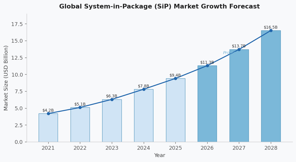
The global SiP market is on a steep growth trajectory. According to industry research, the market was valued at approximately $8 billion in 2024 and is forecast to approach $17 billion by 2028, growing at a compound annual rate exceeding 15%. Several macro trends are powering this expansion:
- IoT and Wearable Devices: The explosion of connected devices demands ultra-compact, low-power modules. SiP allows designers to integrate sensing, processing, and connectivity functions into a package small enough for a smartwatch or medical implant.
- 5G and Advanced Communications: Millimeter-wave 5G systems require highly integrated RF front-end modules. SiP enables the co-packaging of RF components with antenna structures, dramatically reducing signal loss and board real estate.
- Defense and Aerospace Miniaturization: Modern defense electronics – from drone guidance systems to soldier-worn electronics – require extreme miniaturization alongside ultra-high reliability under harsh environmental conditions.
- Medical Device Innovation: Implantable devices, hearing aids, and continuous health monitors are pushing miniaturization to new extremes, where SiP technology enables life-critical functionality in sub-centimeter packages.
- Automotive Electronics: Advanced driver-assistance systems (ADAS) and autonomous vehicle platforms require high-density, thermally reliable SiP modules capable of operating across extreme temperature ranges.
The Technical Challenges of SiP Design and Manufacturing
While SiP offers compelling advantages, its design and manufacturing complexity is substantial. Engineers face a constellation of technical challenges that require deep, cross-domain expertise:
- Thermal Management: Integrating multiple high-power components into a small package concentrates heat significantly. Ensuring reliable thermal dissipation without increasing package height or weight requires sophisticated substrate engineering, embedded coin technology, and careful die placement.
- Signal Integrity and Electromagnetic Interference (EMI): Heterogeneous integration creates complex signal routing challenges. Fine-pitch interconnects between dies must maintain controlled impedance while minimizing crosstalk and EMI – particularly critical in RF and high-speed digital applications.
- CTE Mismatch: Different materials – silicon dies, organic substrates, and passive components – expand and contract at different rates under thermal cycling. Managing coefficient of thermal expansion (CTE) mismatches is essential for long-term reliability, especially in aerospace and defense applications where temperature extremes are the norm.
- Supply Chain Complexity: Traditional SiP development requires coordinating multiple specialized vendors for substrate fabrication, die sourcing, assembly, and testing. Each handoff introduces risk, delay, and potential quality variation.
- Design for Testability: Testing a fully assembled SiP module is fundamentally more difficult than testing individual components. Embedded dies and multi-layer substrates limit physical access, requiring sophisticated In-Circuit Testing (ICT) and system-level test strategies.
The Landscape of SiP Solutions Today
The market has responded to SiP complexity in several ways. Large Outsourced Semiconductor Assembly and Test (OSAT) companies offer high-volume SiP assembly, but their minimum order quantities and standardized processes are often mismatched with the prototype-to-mid-volume needs of defense, aerospace, and medical device companies. Dedicated substrate foundries provide advanced substrate technology but require separate assembly and test partners, fragmenting the supply chain.
The result is that many engineering teams face a frustrating choice: accept the limitations of standardized, high-volume OSAT services, or manage a complex multi-vendor supply chain that introduces quality risk and schedule uncertainty. A third path – working with an integrated, all-in-one solutions provider – is increasingly recognized as the most effective approach for complex, high-reliability SiP programs.
For a deeper understanding of the academic and technical foundations of SiP development, the IEEE Xplore library provides extensive peer-reviewed research on heterogeneous integration, organic substrates, and advanced packaging reliability testing.
How an All-in-One Approach Addresses SiP Complexity
PCB Technologies, with its specialized iNPACK division, has built an integrated capability that directly addresses the core challenges of SiP development. As described on their website, the company is an “All-in-One Solutions Provider of Miniaturization & Advanced IC Packaging Solutions,” operating with a single-roof approach that spans design, substrate fabrication, package assembly, and testing.
Their iNPACK division offers advanced System-in-Package solutions as multi-component, multifunction products. Key capabilities include size reduction, high thermal conductivity, ultra-thin substrates with fine lines and spacing, controlled CTE, 3D design, shielding options, sealing solutions, fine-pitch flip-chip and copper pillar technology, double-side assembly, development and production testing, and full turnkey solutions.
A core differentiator of iNPACK is its organic substrate technology, supporting 25-micron lines and 25-micron spacing – precision that enables the fine-pitch signal routing critical to advanced SiP applications. Their on-site, certified cleanroom manufacturing facility ensures that sensitive components remain free from contamination throughout the assembly process.
Critically, PCB Technologies’ approach eliminates the multi-vendor fragmentation that plagues many SiP programs. Their R&D center is located within the same complex as their manufacturing facilities, enabling seamless transitions from design iteration to prototype production without the handoff delays and communication gaps inherent in fragmented supply chains.
For engineers exploring panel level packaging as an alternative to wafer-level processes, iNPACK’s panel-level approach uses rectangular panels similar to organic substrate manufacturing – designed for efficient production, lower cost per unit, and the flexibility to incorporate Multi-Chip Module (MCM) and SiP assembly on the same production infrastructure.
SiP in Practice: Applications Across High-Demand Industries
The industries best positioned to leverage SiP technology share a common need: maximum functionality in minimum space, with uncompromising reliability. PCB Technologies serves customers across medical, defense, aerospace, communications, and semiconductor sectors – all of which are increasingly turning to SiP as a strategic platform.
- Defense Electronics: Miniaturized radar modules, electronic warfare systems, and soldier-worn communications devices require SiP solutions that maintain performance under shock, vibration, and extreme temperatures. High-reliability SiP with embedded thermal management meets these requirements.
- Medical Devices: From cochlear implants to continuous glucose monitors, medical SiP modules must combine RF, sensing, and processing in biocompatible packages that meet ISO 13485 quality standards – a certification held by PCB Technologies.
- IoT and Industrial Systems: Industrial IoT nodes that operate in harsh environments require rugged SiP modules with wide operating temperature ranges, integrated sensing, and low-power wireless connectivity.
Conclusion: SiP Is No Longer Optional — It Is a Strategic Imperative
System-in-Package technology has moved from a niche solution for space-constrained applications to a mainstream platform technology across multiple high-growth industries. For product teams facing the dual pressure of miniaturization and performance, SiP is increasingly the answer – but only when implemented with the right combination of substrate expertise, assembly precision, and integrated design-to-test capability.
The companies that will lead in the next wave of electronics miniaturization will be those that choose manufacturing partners capable of delivering SiP solutions as an end-to-end, accountable service – from substrate design through final system testing, all under one roof.
Summary: IC interconnect technology – how a semiconductor die connects electrically to its substrate or package – is one of the most consequential decisions in modern electronics design.
This article examines: the technical fundamentals of wire bonding and flip chip packaging; the market trends reshaping interconnect technology choices; the engineering tradeoffs that determine which approach is optimal for a given application; the landscape of available solutions; and how an integrated packaging capability enables engineers to access both technologies – and choose freely between them – within a single supply chain.
For engineers evaluating interconnect strategies for their next design, understanding the full depth of wire bonding options and their flip chip alternatives is essential. The choice directly affects device performance, package size, signal integrity, manufacturing cost, and qualification timeline.
The Fundamentals: What Wire Bonding and Flip Chip Actually Are
At its core, the IC interconnect challenge is straightforward: a semiconductor die contains hundreds or thousands of tiny electrical contact pads. Those pads must be connected to the package substrate – which then connects to the PCB – with minimal resistance, inductance, and crosstalk, while maintaining mechanical integrity through thermal cycling, vibration, and shock.
Wire Bonding is the oldest and most widely used interconnect technique. Thin wires – typically gold, copper, or aluminum – are bonded from the die bond pads to the package substrate using thermal compression, ultrasonic energy, or a combination of both (thermosonic bonding). The resulting wire loops are visible under a microscope as delicate arcs spanning from die to substrate.
Flip Chip packaging inverts this approach. Instead of bonding wires from the top surface of the die, the die is flipped face-down, with solder bumps or copper pillars on the active surface connecting directly to matching pads on the substrate. The entire connection is made through these bumps in a single reflow step, with no wire loops.
Market Trends: The Steady Rise of Flip Chip
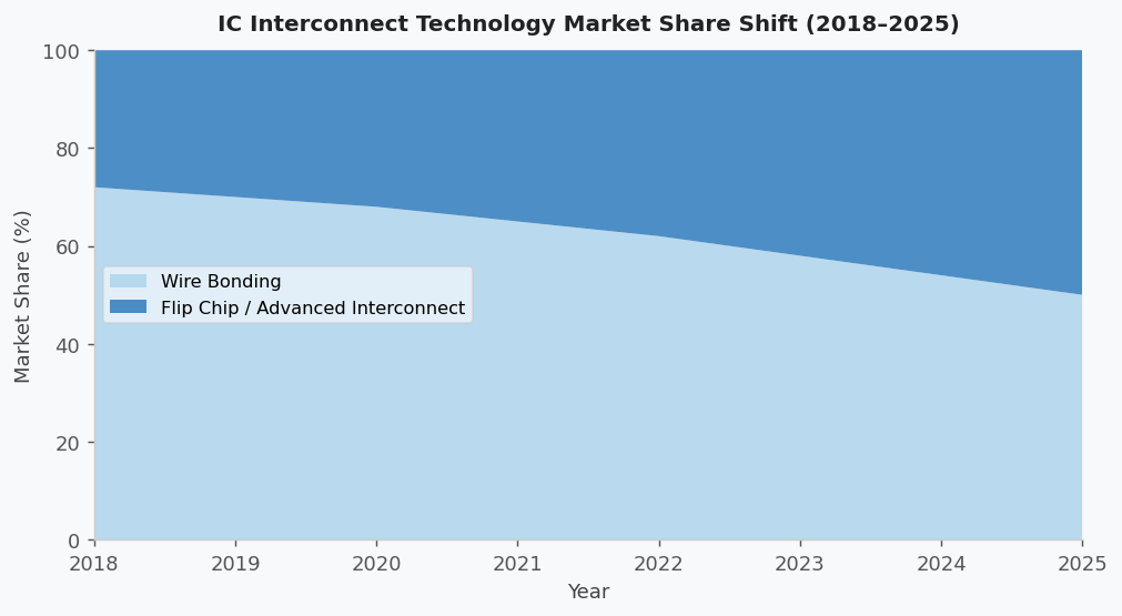
The global IC packaging market is undergoing a structural shift away from wire bonding as the dominant interconnect approach, driven by the performance demands of advanced applications. Industry research indicates that flip chip packaging now accounts for roughly half of the total IC interconnect market by value, with penetration continuing to grow in high-performance segments.
Several converging trends are driving this shift:
- High-Speed Digital Performance: Modern processors, memory controllers, and network chips operate at speeds where wire inductance – an inherent characteristic of wire bond loops – causes signal integrity problems. Flip chip’s shorter, lower-inductance interconnects are essential for chips operating above a few gigahertz.
- Fine-Pitch I/O Requirements: As die complexity increases, the number of I/O connections grows and their pitch shrinks. Advanced chips now require hundreds to thousands of I/O connections at pitches that wire bonding cannot reliably achieve, but flip chip copper pillars can support.
- Thermal Performance: Flip chip’s inverted die placement exposes the back side of the silicon directly upward, enabling direct attachment of a heatsink to the die – dramatically improving thermal dissipation compared to wire bonded packages where the die back faces the substrate.
- Package Height Reduction: Wire bond loops require vertical clearance above the die. Flip chip eliminates this requirement, enabling ultra-thin packages critical for wearables, implantable medical devices, and ultra-thin consumer electronics.
Where Wire Bonding Remains the Optimal Choice
Despite the growth of flip chip, wire bonding is far from obsolete – and for many applications, it remains the technically and economically optimal choice.
- Cost-Sensitive, Standard I/O Applications: Wire bonding equipment and processes are mature, widely available, and highly cost-effective for chips with moderate I/O counts and standard pitch. For commodity sensors, microcontrollers, and discrete semiconductors, wire bonding delivers excellent performance at minimal cost.
- Mixed-Die Assemblies: In multi-chip module (MCM) designs and System-in-Package (SiP) assemblies, wire bonding enables flexible interconnection between dies of different sizes and heights – including die-to-die connections within the same package that would be impractical with bump-based approaches.
- Known-Good Die (KGD) Management: Wire bonding can be performed after functional testing of individual dies, reducing the risk of assembling expensive SiP modules with defective components.
- Rework Capability: Wire bonds can be selectively reworked – broken bonds can be re-bonded – providing a repair option that flip chip assemblies generally do not offer, which is valuable in low-volume, high-value applications.
Flip Chip vs. Wire Bond: The Engineering Decision Framework
The choice between flip chip vs wire bond is not a binary decision with a universal right answer. It is a multi-dimensional optimization across performance, cost, form factor, reliability, and supply chain complexity. The key decision drivers include:
- Operating Frequency: For applications below approximately 1 GHz, wire bonding is typically sufficient. For RF, mmWave, and high-speed digital applications above a few GHz, flip chip’s lower parasitics become essential.
- I/O Count and Pitch: For designs with more than a few hundred I/O at fine pitch, flip chip or copper pillar technology is generally required. Wire bonding becomes physically impractical at very high I/O densities.
- Package Thickness: For applications where vertical space is at a premium, flip chip eliminates the wire loop height overhead – typically 200–400 microns – enabling thinner packages.
- Thermal Requirements: High-power dies benefit significantly from the superior thermal path provided by direct heatsink attachment enabled by flip chip orientation.
- Volume and Cost Sensitivity: At low-to-medium volumes, wire bonding is typically more cost-effective. At high volumes, the economics become more application-specific and are influenced heavily by substrate cost, yield, and test strategy.
The Integration Advantage: Access to Both Technologies in One Supply Chain
One of the most underappreciated challenges in advanced IC packaging is the supply chain fragmentation that results when different interconnect technologies require different vendors. Many organizations source wire bonding from one assembly house, flip chip from another, and organic substrates from a third – creating a coordination burden that adds time, cost, and quality risk to every program.
PCB Technologies, through its iNPACK division, offers a fundamentally different model. As described in their materials, the iNPACK division provides complete package PCB assembly solutions including SiP design and manufacturing, surface mount technology, chip on board (COB) wire bonding, microfabrication, and substrate design and manufacturing – all under one roof.
Their substrate technology supports 25-micron lines and 25-micron spacing, enabling the fine-pitch routing required for both advanced wire bond fan-out designs and flip chip copper pillar interconnects. Their cleanroom manufacturing facility, certified to ISO 9001, ISO 14001, ISO 13485, and AS 9100, ensures the contamination control and process discipline required for reliable advanced interconnects.
For engineers seeking academic grounding in IC interconnect technologies, IEEE Xplore provides extensive peer-reviewed literature on wire bonding reliability, flip chip process development, and advanced packaging interconnect performance – an essential reference for teams evaluating interconnect technology choices.
The Path Forward: Heterogeneous Integration
The most sophisticated packaging programs today do not choose between wire bonding and flip chip – they use both, strategically, within the same SiP module. A high-power processor might use copper pillar flip chip interconnects for maximum performance, while peripheral functions such as a power management IC, a sensor die, or an RF module are wire bonded to the same substrate.
This heterogeneous integration approach requires the substrate to accommodate both interconnect types simultaneously, with the DfM expertise to ensure that both are manufacturable, testable, and reliable at production scale. It is a capability that demands deep, integrated expertise across substrate design, interconnect technology, assembly process, and test engineering.
Conclusion: The Right Interconnect for the Right Application
Wire bonding and flip chip packaging represent complementary – not competing – technologies in the modern IC packaging toolkit. The engineering challenge is not to choose one universally, but to understand each application’s specific requirements deeply enough to select the right approach, and to partner with a manufacturing organization capable of executing either strategy with equal precision and accountability.
As miniaturization continues to advance and new application categories – implantable medical devices, next-generation defense electronics, advanced automotive systems – push the boundaries of what is possible, the ability to access both interconnect technologies through a single, integrated supply chain will increasingly determine which organizations can deliver on their design intent.
Health And Beauty
Geneo+ vs. Oxygeneo: A Comparative Analysis
In the ever-evolving world of skincare, finding the right treatment for your skin can be a daunting task. Among the innovative solutions available, Geneo+ and Oxygeneo stand out as popular choices for those seeking rejuvenated, youthful skin. But how do these treatments differ, and which one is truly the best option for you? In this comprehensive analysis, we will delve into the unique features, benefits, and outcomes of Geneo+ and Oxygeneo. Whether you’re looking to enhance your skincare routine or simply curious about the latest in facial treatments, understanding these options will empower you to make an informed decision for your skin’s health and beauty. Join us as we explore the ultimate showdown between Geneo+ and Oxygeneo, and discover which treatment reigns supreme in delivering radiant results.
Geneo+ and Oxygeneo are both innovative facial rejuvenation technologies that offer a range of benefits for improving skin health and appearance. While they share some similarities, there are key differences between the two technologies.
Geneo+
Geneo+ is a three-in-one facial treatment that combines exfoliation, oxygenation, and nutrient infusion. It uses a unique capsule technology to deliver oxygen and nutrients to the skin while simultaneously exfoliating dead skin cells. Geneo+ also incorporates radiofrequency (RF) technology to stimulate collagen production and improve skin elasticity.
Oxygeneo
Oxygeneo is another innovative facial treatment that combines exfoliation, oxygenation, and infusion. It uses a patented technology to infuse oxygen and nutrients into the skin while gently exfoliating. Oxygeneo also offers the option of adding a variety of serums to target specific skin concerns.
Key Differences Between Geneo+ and Oxygeneo
| Feature | Geneo+ | Oxygeneo |
| Capsule Technology | Yes | No |
| Radio Frequency (RF) | Yes | No |
| Customizable Serums | No | Yes |
| Exfoliation Method | Mechanical | Chemical |
Benefits of Geneo+ and Oxygeneo
Both Geneo+ and Oxygeneo offer a range of benefits, including:
- Improved skin texture: Both technologies can help to refine pores and smooth the skin’s surface.
- Enhanced skin radiance: By removing dead skin cells and increasing oxygenation, both treatments can help to brighten the complexion.
- Reduced appearance of fine lines and wrinkles: The RF technology in Geneo+ and the nutrient infusion in both treatments can help to improve skin elasticity and reduce the appearance of aging signs.
- Hydrated skin: Both treatments can help to improve skin hydration and plumpness.
Choosing the Right Treatment
The best treatment for you will depend on your specific skin concerns and preferences. It is recommended to consult with a qualified skincare professional to determine which technology is most suitable for your needs.
In conclusion, both Geneo+ and Oxygeneo offer innovative and effective facial rejuvenation treatments. While they share some similarities, there are key differences between the two technologies. By understanding these differences, you can make an informed decision about which treatment is right for you.

Edge AI Explained: How On-Device AI Processing Is Replacing the Cloud
The Rise of System-in-Package (SiP): How Advanced IC Packaging Is Redefining Electronics Miniaturization
Wire Bonding vs. Flip Chip: Navigating the Evolving World of IC Interconnect Technology

-
Business Solutions2 years ago
Understanding A2P Messaging and the Bulk SMS Business Landscape
-

 Business Solutions2 years ago
The Power of Smarts SMS and Single Platform Chat Messaging
-

 Business Solutions2 years ago
Exploring OTP Smart Features in Smart Messaging Services
-

 Business Solutions2 years ago
Live Video Broadcasting with Bonded Transmission Technology
-

 Business Solutions1 year ago
The Future of Healthcare SMS and RCS Messaging
-

 Business Solutions2 years ago
2-Way Texting Solutions from Company Message Services
-

 Business Solutions2 years ago
Communication with Analog to Fiber Converters & RF Link Budgets
-

 Business Solutions2 years ago
B2B vs. B2C Content Creation: Tailoring Your Message to Win the Deal